


Japanese Semiconductor Firms Explore Collaboration in Dholera to Strengthen India’s Chip Ecosystem
Dholera, India – In a significant boost to India's semiconductor ambitions, a delegation of 20 Japanese semiconductor ecosystem support companies visited Dholera Special Investment Region (SIR) this week. The delegation included senior representatives from globally reputed firms such as Shimizu Corporation, Japan, known for its expertise in infrastructure and precision engineering. The delegation’s Dholera visit followed SEMICON India 2025, the event where India highlighted policy support and fiscal incentives to attract global players in chip manufacturing. India’s policy framework but also in on-ground execution and readiness.
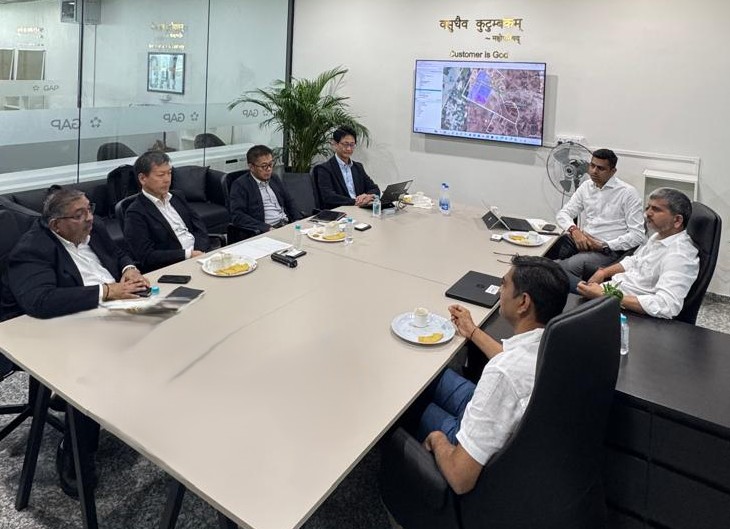
At the ABCD Building, the administrative hub of Dholera, the Project office of GAP Group, the Shimizu Corporation officials held discussions with GAP Group, one of western India’s fastest-growing infrastructure developers and the first-mover real estate and infrastructure developer in Dholera’s Activation Zone. The talks centered on leveraging Japan’s technological know-how alongside India’s scale and talent pool, supported by Dholera’s world-class smart city infrastructure, to strengthen Dholera emerge as a semiconductor hub. India’s largest semiconductor fabrication facility, a joint venture of the Tata Group and Taiwan's PSMC, is already taking shape in Dholera.
Japan holds a key position in the global semiconductor supply chain, contributing leadership in chip-making equipment, specialty gases and materials, and advanced components. For India, collaboration with Japan is vital to build a resilient and competitive semiconductor hub.
For the visiting delegation, GAP Group presented solutions spanning industrial parks, residential and hospitality projects, and leasing services, effectively offering a one-stop partner for smooth market entry. Projects showcased included Akhilam Township, Greenera Garden Villa near the Tata Semiconductor Fab, Avant with 1,000 premium units, Aakar Premium Studio Apartments, and the GAP Industrial Park, which has 40,000 sq mt of ready industrial space in the Activation Zone.
Ambrish Parajiya, Managing Director, GAP Group, said, “The visit of the Japanese semiconductor ecosystem companies to Dholera is a vote of confidence in India’s vision and Dholera’s readiness. Japan brings unmatched precision and reliability, while India offers scale and a huge market. At GAP Group, we are committed to supporting the strategic and longstanding partnership between the two nations with world-class infrastructure to ensure Dholera becomes India’s Semiconductor City.”
The delegation explored multiple areas of collaboration with GAP Group, including setting up precision facilities for Japanese SMEs supplying to Tata Semiconductor and other fabs and deploying GAP Group’s premium studios and villas to host expats, managers, and engineers. The talk also included construction of warehouses, gas distribution systems, and clean rooms in collaboration with Japanese firms and joint skill development programs to train engineers and technicians in semiconductor manufacturing.
Dholera is located 110 km from Ahmedabad, along the Delhi–Mumbai Industrial Corridor. Spread across 927 sq km, it is India’s first Platinum Greenfield Smart City. The region’s strategic location and connectivity via the upcoming Ahmedabad–Dholera Expressway and the under-construction international airport, expected to begin operations by December 2025, also add to its appeal among investors.
The INR 92,000 crore Tata Electronics fab is expected to commence production by 2027 and generate thousands of jobs. Major projects of Renew Energy, INOX Air, Polycab, and a 5GW solar park are also taking shape in the Dholera Activation Zone, projected to create over 1.5 lakh jobs by 2030.
Image Source: GAP Group

 Facebook
 Linkedin
 Subscribe