

Semiconductors: Tapping Sunrise Opportunities
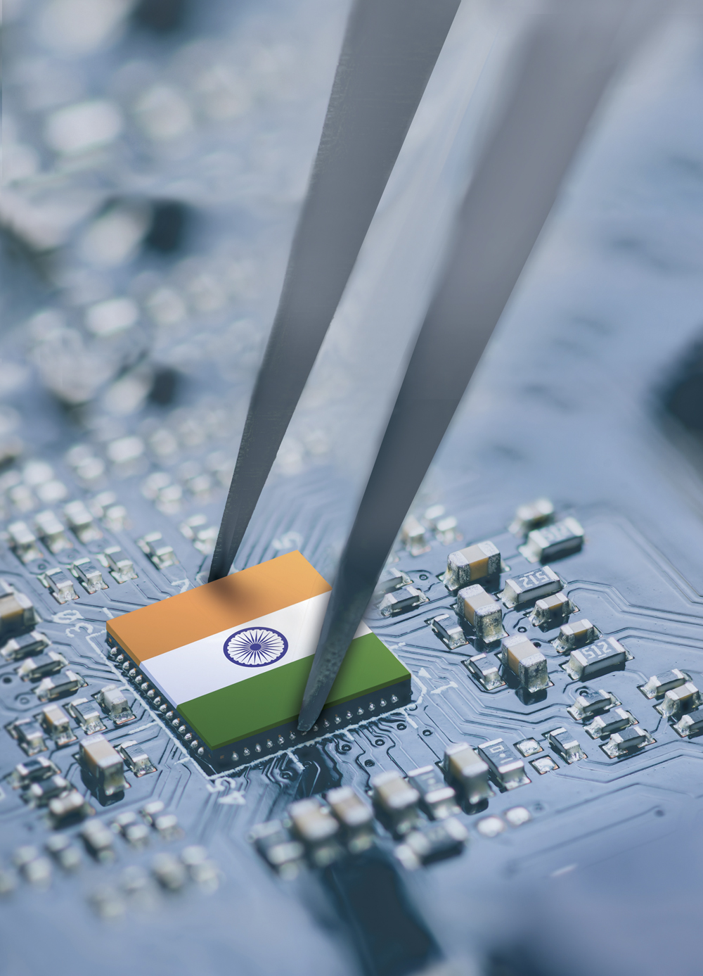
Semiconductors are the heart and brain of all modern electronics and information and communications technology products. They are critical for almost all sectors of the economy now, ranging from automobiles, consumer electronics, communications, clean energy, defense, IT, etc.
The transistor, when it was first invented in 1947, was approximately the size of a large packet of cigarettes. Seventy-five years later, technology has evolved at such a rapid pace that today, a chip the size of a postage stamp can effectively contain the computing power of one billion transistors.
Professor N Ramesh Babu, V Balaraman Institute Chair and Professor of Mechanical Engineering, IIT-Madras, says, “Almost all consumer goods, capital goods, and engineering products are controlled by computers, either embedded or separate units. When we move on to smart manufacturing with the Internet of Things (IoT) and Internet of Services (IoS), the import of semiconductor-based devices like electronic chips comes at a high cost.”
Anil Bharadwaj, Managing Director, Mazak India, opines, “The development of IoT technology, advancements in smartphones, tech-driven modern-day automobiles, and multiple emerging cutting-edge technologies have significantly contributed to the importance of semiconductors in our digital world. Additionally, 5G technology is expected to further contribute to the demand for semiconductors. Increased online traffic is also effectively bound to increase the role of semiconductors and semiconductor equipment in the near future.”
India currently imports all chips, and its consumption of semiconductors is expected to grow from US$24 billion to US$80 billion by 2026 and US$110 billion by 2030.
He adds, “Between 2016 and 2021, internet users increased by 1.3 billion, and in the same period, internet speeds nearly doubled. This trajectory is expected to see exponential growth in the future, which calls for advances in semiconductor production. Even today, tens of millions of extremely small circuits are written on just a 1 cm x 1 cm (0.4 x 0.4 in) square semiconductor chip. As the number of circuits that can be written on a unit area is approaching its limit, manufacturing now calls for innovative solutions. Semiconductor manufacturers are now working to achieve 3D (multilayer) chips. 3D NAND flash memory is the most-advanced semiconductor today. It has a thickness of fewer than 10 µm (0.0004 in) and contains a 64-layer structure. It is believed that the structure will have more than 100 layers in the future. This worldwide trend is likely to influence India as well. In the next decade, we can expect to see advanced semiconductors opening newer avenues for their manufacturing.”
India currently imports all chips, and its own consumption of semiconductors is expected to grow from US$24 billion currently to US$80 billion by 2026 and to US$110 billion by 2030.
However, the exponential demand globally has outstripped the supply, creating a global chip shortage. In India, the Automotive industry faced a huge backlog of orders, and customers had to wait for months to get the delivery of cars.
Other than the Automotive industry, sales in 169 sectors, including computers, mobile phones, and healthcare equipment, were affected by the global chip shortage.
Realizing the importance of the Semiconductor industry, the Government of India has announced a `76,000 crore Production Linked Incentive (PLI) Scheme to encourage semiconductor manufacture in India.
Realizing the importance of the Semiconductor industry, the Government of India has announced a `76,000 crore Production Linked Incentive (PLI) Scheme to encourage semiconductor manufacture in India.
In 2021, the Ministry of Electronics and Information Technology (MeitY) also launched the Design Linked Incentive (DLI) Scheme to incentivize Indian companies involved in semiconductor design and nurture and facilitate them to achieve a turnover of more than `1,500 crore in the next five years.
On the future of the semiconductor business in India, Prasanth Sakhamuri, Director, ASM-HHV Engineering, says, “Semiconductor manufacturing is still very nascent in India. To build semiconductors at any time, India should also be able to manage the production tools and build parts of the tools, if not the whole. Today, we lack the ecosystem for this critical capability. With the strong initiative taken by the Government to have semiconductor manufacturing in the country, we will soon get one- or two-generation old technology being installed. This will help start the build-up of the ecosystem, be it people, services, packaging, etc. The next stage will be to establish the capability to maintain and service the various tools and equipment. This will be the seed of a manufacturing program to develop equipment and fully understand the process. Equipment building without having a detailed understanding of the process is not meaningful. Process technology and equipment technology should go hand in hand. In the next ten years, we will have quite a few semiconductors made in India and make some equipment in the country. They may not be state-of-the-art, but they will reduce our import bill significantly. As the ecosystem evolves, we will be progressing from part-time tool manufacturers and maintenance specialists to full-time tool designers.”
In 2021, MeitY also launched the Design Linked Incentive (DLI) Scheme to incentivize Indian companies involved in semiconductor design and facilitate them to achieve a turnover of over `1,500 crore in the next five years.
Premier educational and research institutions are also playing their part. Professor Babu says, “IIT-Madras, IISc, and a few other IITs have together developed a test bed for 5G technologies. The role of semiconductor devices and systems is crucial if 5G and 6G technologies have to be proliferated to benefit industries like capital goods, FMCG, engineering products, etc. by way of operated assisted manufacture, efficient manufacturing, decision making for smart manufacturing, etc.” Semiconductor equipment manufacture in India
Several Indian companies are now rushing to participate in what is considered a sunrise industry for India.
Rabindra Srikantan, Board Member of the recently-formed joint venture ASM-HHV Engineering, says, “ASM and HHV have expertise in designing and manufacturing sub-systems, components, and providing field support. We decided to form this joint venture ASM-HHV Engineering to capitalize on over 60 years of experience in design, engineering, and manufacturing. Our JV is India’s first for this sector.”
Sakhamuri adds, “Solar is one of the key focus areas in the Indian semiconductor space. It is receiving a significant amount of Government support for the semiconductor policy. The manufacturing of solar cells needs a lot of specialized production tools that are synergic with the capabilities of ASM-HHV. ASM-HHV will also be working towards developing and producing many pieces of equipment, sub-assemblies, and subsystems required to support the establishment of amorphous silicon- and perovskite-based solar cell manufacturing capabilities. In addition, in the Semi space, we will also be working on supporting international companies in obsolescence management and sustaining processes that are not directly supported by the OEMs. We also have plans of establishing a full ecosystem which will be backbone support to the nascent semi industry in India and grow with it.”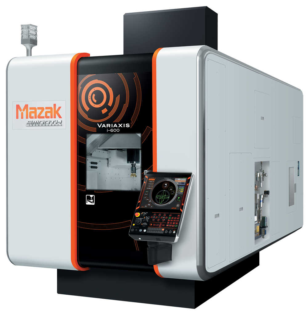 Role of machine tools in the semiconductor industry
Modern-day CNC machines play a vital role in semiconductor machining, and high-precision machines enable manufacturers to maintain extremely tight tolerances on surface finishes, flatness, positional tolerances, etc. that semiconductor components and sub-assemblies require. There is also a wide range of materials that are exceptionally challenging to machine and manufacture.
There are a number of opportunities in the Semiconductor industry, both in India and globally, for the Machine Tool sector.
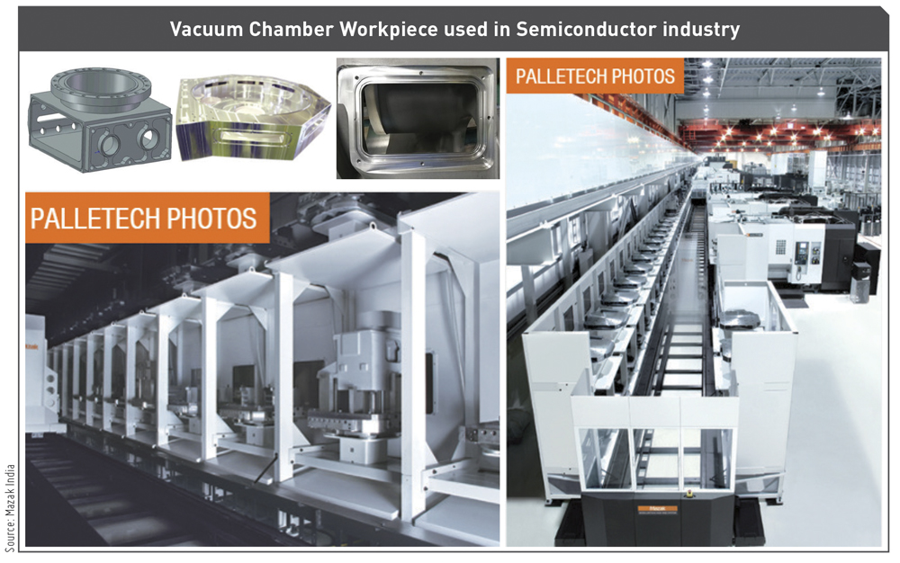
Bharadwaj says, “The vacuum-related units used in semiconductor manufacturing equipment need to have high durability in addition to functioning at a high level. Many of the parts used in such units are machined, and Mazak machine tools are deeply involved in the production process. A turbomolecular pump has an internal structure of many layers or turbine blades, similar to a jet engine, which has to withstand a rotation speed of tens of thousands of revolutions per minute. The turbine blade has a complicated shape, and its machining takes a long time. To machine it, the VARIAXIS and other 5-axis machining centers are effectively used. Vertical Machining Centers, such as the SVC with a high-speed linear motor-driven X-axis, are used to reduce the machining time.
He continues, “Mazak machine tools are also used to machine parts of the table positioning units for wafers, transfer arms, and other units. In addition to metal cutting machine tools, the Mazak hybrid multi-tasking machine with friction stir welding technology, the FJV-60/80 FSW, can be used to machine backing plates (cooling boards), which contributes to the integration of the process phases.”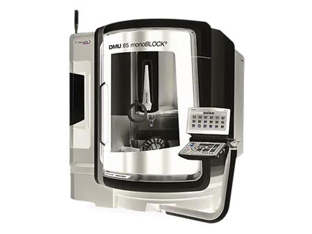 Mazak products are effectively used to improve not only the machining efficiency of the individual machines but also the efficiency of the production process as a whole through the transformation of the plant into a smart factory. Furthermore, the products equipped with Mazak SMARTBOXTM and Smooth Monitor AX contribute to the strengthening of cybersecurity as well as the visualization and analysis of machine operation data. While semiconductors usually attract attention in many fields, the evolution of their manufacturing process deeply involves mechanical engineering and Mazak’s reliable technology to continuously increase productivity.
On Mazak’s plans for India, Bharadwaj shares, “Mazak machines have continued to streamline semiconductor manufacturing the world over. Mazak India has been at the forefront of supplying advanced technological solutions to Indian customers. We have already started working with some of the big players in India and shall be supplying our multitasking machine along with HMC and Palletech systems for unmanned operations.”
Bernd Dötterl, Sales Director - Semiconductor Industry, Deckel Maho Pfronten, says, “The digital future will continue to grow exponentially, and our company DMG Mori is expecting our highest-ever orders from the Semiconductor business in 2022. For machine makers, the advantage is that the machines for chip production are very prone to wear and tear, and therefore, in addition to the new machines, there is an enormous need for spare parts. We are already doing very well in the Semiconductor business and are preparing ourselves over the next one or two years for the next boom in new chip technologies.”
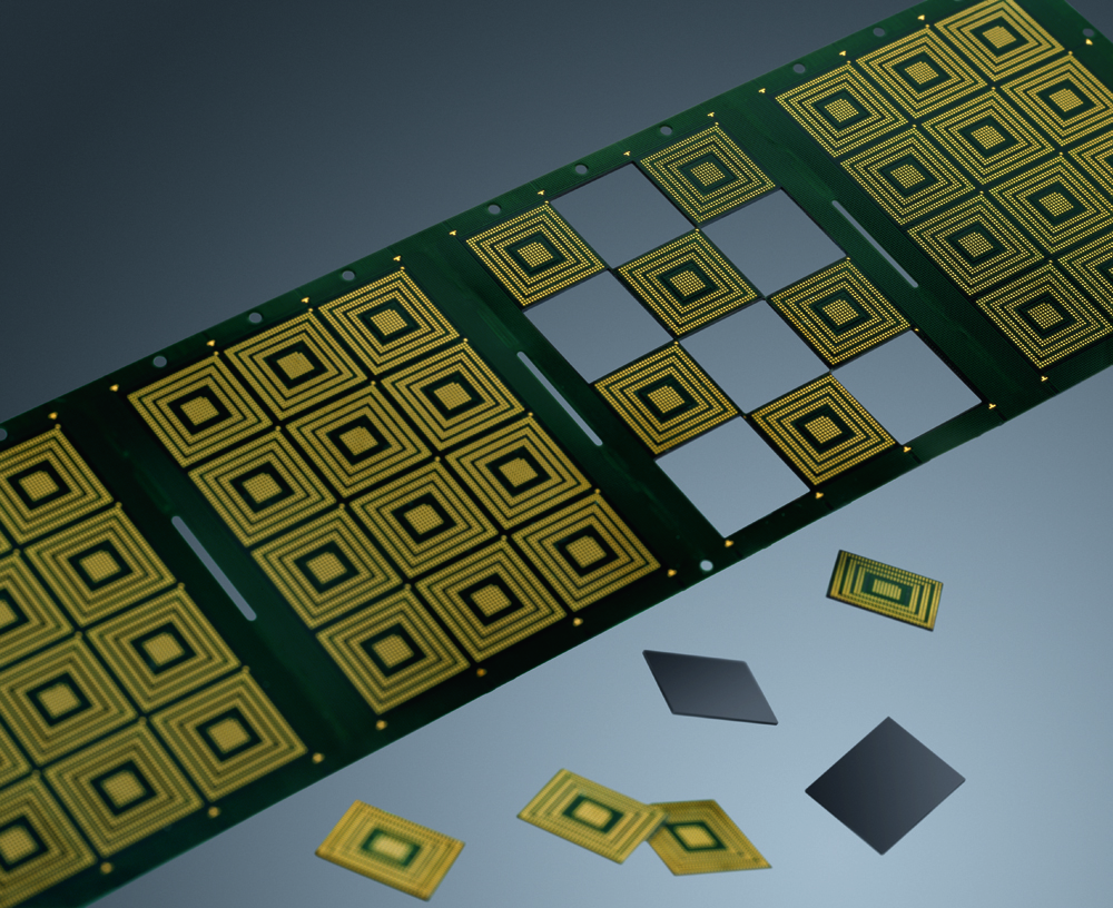
Laser cutting of matrix lead frames
On the plans for the Indian Semiconductor industry, Jose Varghese, Director – Technology, DMG Mori India, says, “DMG Mori has founded a Semiconductor Excellence Center in the year 2022 under the leadership of Bernd Dötterl (classical milling solutions) and Benedikt Brocks (ULTRASONIC solutions). That means we have specified people concentrating on solutions only for Semiconductor customers regarding machine adaptations, special options, technology cycles, and technology. We have a wide range of high-technology machines with a 600 mm to 6 m travel range. We also have multi-tasking machines for milling, turning, and grinding on one machining center."
Between 2016 and 2021, internet users increased by 1.3 billion, and in the same period, internet speeds nearly doubled. This trajectory is expected to see exponential growth in the future, which calls for advances in semiconductor production.
Dötterl says, “DMG Mori has different levels of machine accuracies from standard to ultra-high accuracies up to 3 µm positioning accuracy. We also have ultrasonic solutions for machining advanced materials like Ceramic, Zerodur, and Quartz. Customization is also one of DMG Mori’s strengths, and it is important to guide our customers regarding the right machining strategies, tools, fixtures, coolant solutions, and software applications. We also have multiple automation solutions to enable 24/7 production.”
As semiconductors become faster, smaller, and more efficient, Laser Technology is also playing a big part in the Semiconductor industry.
Pradeep Patil, Managing Director, TRUMPF India, says, “A trend toward miniaturization and extremely large quantities of chips are two of the most important characteristics of the Electronics industry. As a result of its unprecedented precision and good automation potential, laser technology can provide industrial solutions to overcome these challenges. TRUMPF lasers play a fundamental role in the production of the latest generation of Semicon chips. Applications of lasers in the Semiconductor industry enable manufacturing processes such as cutting and drilling silicon wafers, printed circuit boards, or entire electronics modules. Also, high-frequency RF generators from TRUMPF Hüttinger provide reliable and precise process energy for coating and etching processes in the production of silicon wafers. TRUMPF lasers produce very high quantities of reproducible and high-quality products that are predestined for the Electronics industry. More than 1,000 ultrashort pulse lasers from TRUMPF work in the production facilities of global industry leaders around the clock, 365 days a year.”
He adds, “TRUMPF provides a machine solution or an individual laser technology package depending on the area of application. In both cases, customers benefit from the TRUMPF Group’s international service network. The development of micro-electronics, and therefore, the basis of today’s computers, control systems, and smartphones, would be inconceivable without laser technology. Logic and storage chips have structures in the nanometer range and can only be produced using complex exposure processes with laser radiation. The conventional approach with UV laser radiation from excimer lasers is increasingly reaching its limits. In the future, it will only be possible to generate smaller structures with even shorter wavelengths up to 13.5 nanometers in the extreme ultraviolet range (EUV). They help to create a luminous plasma, which delivers extreme ultraviolet radiation (EUV) exposure to the substrate.”
As semiconductors become faster, smaller, and more efficient, laser technology is also playing a big part in the Semiconductor industry.
TRUMPF has developed an internationally unique CO2 laser system in close cooperation with renowned partners—ASML, the largest manufacturer of lithography systems in the world. It has served as an integrator and delivered the components for droplet creation and the scanner. The EUV optics are being supplied by Zeiss. These components make it possible to process more than 100 substrates an hour, enough for series production. This makes EUV lithography not only technical but also a complete commercial success for chip manufacturers worldwide.
Patil says, “In the future, TRUMPF EUV laser technology will make its way into many high-performance chips. The plasma generators from TRUMPF Hüttinger play a fundamental role in manufacturing chips, as the quality of the power supply dictates the quality and precision of the plasma generated. This plasma is used in the next step for doping (ion implantation), deposition (PECVD, ALD), or removal (plasma etching) of different materials for the production of semiconductor chips. During this process, toxic environmental gases are generated, which are effectively cleaned by a special system in the TRUMPF Hüttinger generators, thus keeping the CO2 footprint in the semiconductor production as low as possible. After exposure and the construction of the circuits on the silicon wafers, the separation into separate chips is the next challenge for the electronic process chain. In order to achieve the smallest possible kerfs and high-edge quality and to avoid damaging the sensitive chips due to thermal influences, ultrashort pulse lasers from TRUMPF are used for separation. These enable the material to be processed without unwanted heat influence and the highest precision as part of the laser processing. These lasers are also suitable for trimming sensitive modules (system-in-package), processing multi-material printed circuit boards, and drilling so-called microvias in silicon and glass. The industry also uses TRUMPF lasers for targeted layer ablation, cutting films, and marking.”
For India, the strategic risk of being left behind in the semiconductor race in a tough geopolitical neighborhood is fraught with danger. The ability to fabricate chips will certainly give India the Aatmanirbhar quotient to power its economy and protect its borders.
The miracle of sunrise
Despite being the second-biggest maker of mobile phones and a multi-billion-dollar electronic goods market, India is an infant in the Semiconductor industry. We are severely handicapped by the vagaries of global supply chains, and our geopolitical equations have also dramatically changed in recent years, with China flexing its muscle globally. China and Pakistan are also working together to forward their own agendas. US Senator Ben Sasse of the US Senate Intelligence Committee says, “Modern wars are fought with semiconductors.”
For India, the strategic risk of being left behind in the semiconductor race in a tough geopolitical neighborhood is fraught with danger. The ability to fabricate chips will certainly give India the Aatmanirbhar quotient to power its economy and protect its borders.
Witnessing a new dawn is one of the most exhilarating sights, and it brings with it new hope for new beginnings. There is a saying that we can only appreciate the miracle of a sunrise if we have waited in the darkness. India has waited far too long for this moment to arrive — a new sunrise beckons.

Reji Varghese
Managing Director
RV Forms & Gears
 Facebook
 Linkedin
 Subscribe