


THE EMERGENCE OF LASERS IN THE DIGITAL AGE
Lasers have become a household name ever since they burnt their way into public consciousness in the famous James Bond movie, Goldfinger, in 1964.
One of the first commercial manufacturing applications using lasers happened in 1965 when the Western Electric Company, US, adapted a pulsed system for the production drilling of diamond wire drawing dies. In this application, the processing time for drilling of a die was reduced from 24 hours using conventional methods to less than one hour with lasers.
A variety of commercial drilling applications have since been developed; one of the most successful being laser drilling of cooling passages in gas turbine parts. The success of these initial production applications hinged on the laser’s ability to accurately deliver a precisely controlled amount of energy to a highly localized region of a workpiece.
Cutting with Fiber Lasers
Fiber lasers emerged in the commercial laser cutting space in 2009. In 2007, the Italian technology company Salvagnini began heavily investing in the development of fiber lasers that could cut sheet metal.
From the 1960s, in just six decades, laser cutting technology has advanced in leaps and bounds with fiber lasers now capable of cutting through steel 100 mm thick. Additionally, recent advances have also made laser cutting machines more affordable and widely available to small businesses.
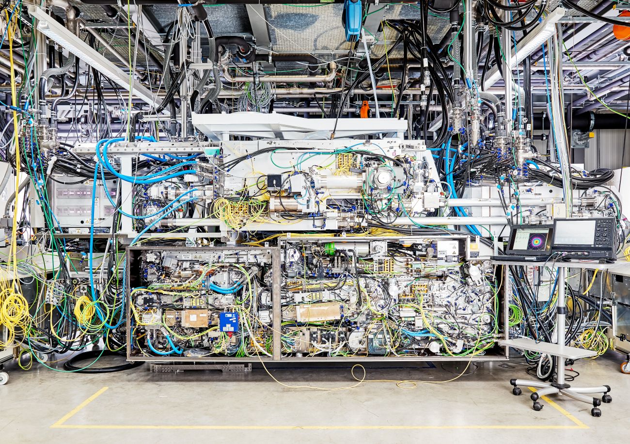
Lasers in Electronics
The buzzwords in the Electronics industry are faster, smaller, and more efficient, with increased miniaturization and production in extremely large volumes. Pradeep Patil, Managing Director, TRUMPF (India) Pvt Ltd, one of the leading laser companies in the world says, “As a result of unprecedented precision and good automation potential, laser technology can provide industrial solutions to these challenges. TRUMPF lasers play a fundamental role in the production of the latest generation of computer chips. Lasers also enable a large number of other process steps to be carried out, such as cutting and drilling silicon wafers, printed circuit boards, or entire electronics modules.”
|
Moore’s law, named after Gordon Moore, one of the Co-founders of Intel, postulates that the
|
Emergence of EUV Laser Technology
EUV or Extreme Ultraviolet Light is an optical lithography technology used in semiconductor device fabrication to make integrated circuits. It uses EUV wavelengths, roughly spanning a 2 percent FWHM bandwidth near 13.5 nm, using a laser-pulsed tin plasma, to produce a pattern by using a reflective photomask to expose a substrate covered by photoresist.
With the advancement of industries like mobile phones, 5G, Industry 4.0, new age medical technology, autonomous driving, artificial intelligence, etc., miniaturization and automation are exponentially increasing the requirements on computer performance.
This requires a lot more transistors to be placed on the semiconductors inside chipsets. In fact, Moore’s law, named after Gordon Moore, one of the Co-founders of Intel, postulates that the number of transistors in a dense integrated circuit doubles about every two years. This law still applies today with semiconductors having integration densities of up to 100 million transistors to one square millimeter.
Patil says, “The size of semiconductor structures is inching closer and closer to atomic dimensions. High-performance laser amplifiers by TRUMPF play a central role in the production of these chips. They help to create a luminous plasma that delivers extreme ultraviolet radiation (EUV) exposure to the substrate. In close cooperation with ASML, the world’s largest manufacturer of lithography systems, as well as Zeiss, the optical systems manufacturer, TRUMPF has developed a one-of-a-kind CO2 laser system which can process over 100 substrates an hour.”
Without laser technology, the development of microelectronics, computers, and smartphones, would be inconceivable as logic and storage chips have structures in the nanometer range that can only be produced using complex exposure processes with laser radiation. The conventional approach with UV laser radiation from excimer lasers is increasingly reaching its limits and in the future, it will only be possible to generate smaller structures with even shorter wavelengths in the EUV range.
EUV Lithography
The Semiconductor industry is constantly looking out for cost-efficient and mass-production technologies to expose even smaller structures on silicon wafers. New-age computer chips that come in nanometer dimensions can only be produced by complex exposure processes with the help of lasers. This is where the conventional approach with UV laser exposure by excimer lasers has its limitations. Smaller structural sizes in ranges of less than ten nanometers can no longer be created with UV laser exposure by excimer lasers. These fragile and intricate structures require exposure to even shorter wavelengths – rays in the EUV range.
Patil says, “The major challenge of EUV lithography is to generate radiation with the optimal wavelength of 13.5 nanometers. The solution: A luminous plasma generated by laser radiation that delivers this extremely short-wave radiation. A generator drops tin droplets into a vacuum chamber, then a pulsed high-power TRUMPF laser impacts the passing tin droplets – 50,000 times per second. The tin atoms are ionized, and an intensive plasma is created. A collector mirror captures the EUV radiation emitted by the plasma in all directions, bundles it, and finally transfers it to the lithography system for exposure of the wafer.”
Tech Talks is a column by industry veteran and journalist Reji Varghese that talks about the latest advancements in Machine Tools, provides snippets from history, interesting facts, etc. about the Machine Tool industry.
 |
Reji Varghese MD RV Forms & Gears fngreji@gmail.com |
Source: TRUMPF Group
 Facebook
 Linkedin
 Subscribe